Brief Introduction of DC Numerically Controlled Adjustable Regulated Power Supply
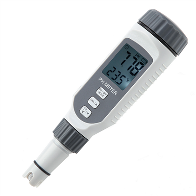
DC stabilized power supply is a commonly used electronic device, which can ensure a stable output voltage when the grid voltage fluctuates or the load changes. A low-ripple, high-precision voltage regulator has important practical application value in the fields of instrumentation, industrial control and measurement. The output voltage range of the regulated power supply given in this design is 0-18 V, the rated operating current is 0.5 A, and it has +, - step voltage adjustment function, the minimum step is 0.05 V, and the ripple is not more than 10 mV , In addition, LCD liquid crystal display can also be used to display its output voltage value.
Introduction
1 System hardware design
The system is composed of a power supply module, a voltage regulation module, a D/A conversion module, a display and a keyboard module, and Fig. 1 shows a block diagram of the structure and principle of the DC NC power supply.
1.1 System power module
The dual 17.5V AC voltage obtained after the 220V mains is stepped down by a 220V/17.5V transformer can be rectified by a full bridge to obtain two voltages of ±21V, one of which +21V voltage is supplied to the regulator tube as a power supply for external output, and the other All the way through the three-terminal voltage regulator 7815 to get +15V, and then through the 7805 to get +5V voltage. The -21V voltage gets -15V voltage through the three-terminal voltage regulator MC7915, which is used as the working power supply of the system itself.
1.2 Voltage adjustment module
The voltage adjustment module circuit in the regulated power supply is shown in Fig. 2 . Among them, the adjustment tube adopts the form of composite tube (composed of Q1 and Q3) to achieve high current output. Since this design requires Iomax=0.5A, Iomin=0A, pm=(Vimax-Vomin)Iomax=(18-0)×0.5 =9W, therefore, the adjustment tube in this circuit can choose TIp41 (its Icmax=6A>Iomax=0.5A; pcw=65W>9W, VCEOmax=100V>18V), of course, 2N5832 can also be used.
The comparative amplification of the circuit is designed with the operational amplifier NE5534, which has the characteristics of high common-mode rejection ratio, fast response speed and high slew rate. When designing, a voltage-dividing sampling circuit can be composed of R10, R11A, and R12, and R10/(R11A+R12)=1/4 is required, that is, when the output
When the voltage exists △UO=0.05V, △Ua=0.04V, which is consistent with the change of the output of DAC (10/255=0.04V=1LSB). In fact, after DAC conversion to convert the current into voltage and amplify the voltage, the obtained 10V voltage can be sent to the non-inverting terminal of the comparator NE54534 as the reference voltage for comparison. Since DAC0832 is an 8-bit D/A converter, it has 255 steps. Thus, when the CpU controls the DAC to vary by 1LSB, the corresponding change in Va is 0.04V, so the adjustable variation of Uout is 0.05V (step size). The negative feedback circuit composed of NE5534, Q1, Q3 and sampling circuit can realize the purpose of adjusting the output voltage (voltage stabilization).
The overcurrent protection in the circuit is completed by R9 and 02. When Io>0.7A, VR9=R9Io≥1×0.7=0.7V, at this time, Q2 is turned on, and shunts the base of the adjustment tube Q3, so that the on-resistance of TIp41 increases and the output voltage decreases, thus achieving over purpose of stream protection. If necessary, a red light-emitting diode can also be connected as an over-current indicator. The short-circuit protection of the system is accomplished by a fuse.
1.3D/A conversion module
The digital-to-analog conversion circuit in this system is shown in Figure 3. It consists of DAC0832, two-stage low-drift operational amplifier μA714 and VREF circuit. DAC0832 and operational amplifier U3A convert the 8-bit binary data sent by CpU into a voltage of 0-5V, and then reversely amplify twice through operational amplifier U3B to obtain a voltage of 0-10V. Therefore, the conversion resolution of the DAC is 10/(28-1)=0.04V, that is, the change of the data output by the CpU to the DAC is 1Bit, and the change of the DAC output voltage is 0.04V. The VREF circuit provides the reference voltage for the DAC, and adjusting R5A keeps the reference voltage at 5V.
1.4 Display and keyboard module
The voltage display and keyboard circuit in this power supply are shown in Figure 4. After the output voltage is limited by R13 and sampled by R14, it can be sent to TLC2453-1 for analog-to-digital conversion. The TLC2453-1 in Figure 4 is an 11-channel, 12-bit serial A/D converter with 12-bit resolution, a conversion time of 10 μs, 11 analog input channels, 3 built-in self-test modes, and a sampling rate of 66 kbps , Linearity error ± 1LSBmax, with conversion result output EOC at the same time, and can be unipolar or bipolar output. Programmable output data length via its programmable MSB or LSB preamble. The clock frequency of TLC2453-1 is 4.1MHz, the sampling signal of the power output voltage Uo is input from IN0, the I/O clock terminal, data input terminal, converted data output terminal and chip selection terminal of the chip are connected with p2.3, P2.2, p2.1, and p2.0 are connected, and then output from p0 port after being processed by the single-chip microcomputer, and then sent to the character liquid crystal display SMC1602A to display the output voltage after being driven by the exclusion 9A472J. In the circuit, the crystal oscillator frequency of AT89S51 microcontroller is 12MHz, and p1.0~p1.3 are connected to the voltage regulating button. When increasing the voltage, call the button S1 coarsely with a step of 1V, call S2 finely with a step of 0.05V; when decreasing the voltage, call S3 coarsely with a step of 1V, and call S4 finely with a step of 0.05V. In this way, the output voltage can be adjusted to the required voltage through their organic combination.