This article will briefly explain the measurement method and gear switching of the digital multimeter resistance voltage range, so that everyone can have a deeper understanding of the measurement principle of the digital multimeter resistance voltage range.
Schematic diagram of resistance test
Figure 1 is an overall schematic diagram of the connection of the resistance gear signal input part when Jinghua Micro SD7890 chip is used as a digital multimeter solution. The resistance to be measured is Rx, and the resistance network inside the chip can provide us with a reference resistance Rr for measuring resistance. When the resistance gear is selected, different resistance networks can be selected to switch different reference resistances. There is no need to build a switch network externally to switch the reference resistance. Therefore, the circuit of the external signal input part is relatively simple, and the hardware cost is greatly reduced.
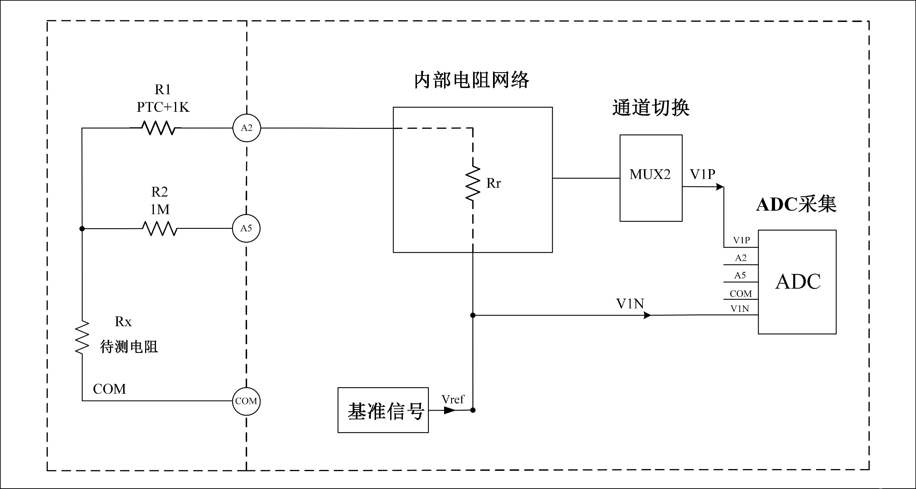
Figure 1. Resistance Measurement Connection Schematic
Principle of Resistance Measurement
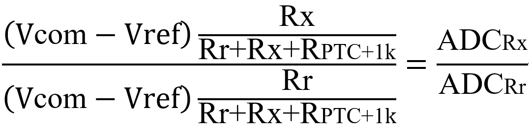
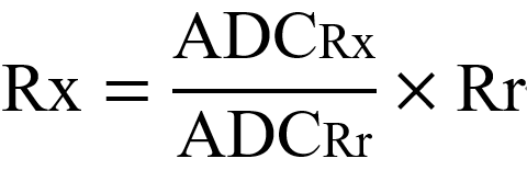
Figure 1 is a schematic diagram of the internal switch network connection of the chip. The principle is to generate a reference voltage Vref from the reference signal, the voltage at the COM terminal is Vcom, the resistance to be measured is Rx, and the internal reference resistance Rr is connected in series to form a loop. The output voltage Vref may be different. One principle is to make the voltage divider on Rx as large as possible, and then use the 24-bit high-precision ADC inside the chip to measure the voltages across the Rx and Rr resistors, respectively, to obtain the code values ADCRx and ADCRr, and then according to the series connection The principle of circuit voltage divider can solve the resistance value of Rx.
The derivation is as follows:
After simplification:
Schematic diagram of voltage test
Figure 2 is the overall schematic diagram of the connection of the voltage range signal input part when Jinghua Micro SD7890 chip is used as a digital multimeter solution. The voltage to be measured is Vin, and the resistance network inside the chip can provide us with the reference resistance Rr of the voltage divider resistance. When different voltage levels are selected, different resistance networks can be selected to switch different reference resistances. There is no need to build a switch network externally to switch the reference resistances. Therefore, the circuit of the external signal input part is relatively simple, and the hardware cost is greatly reduced.
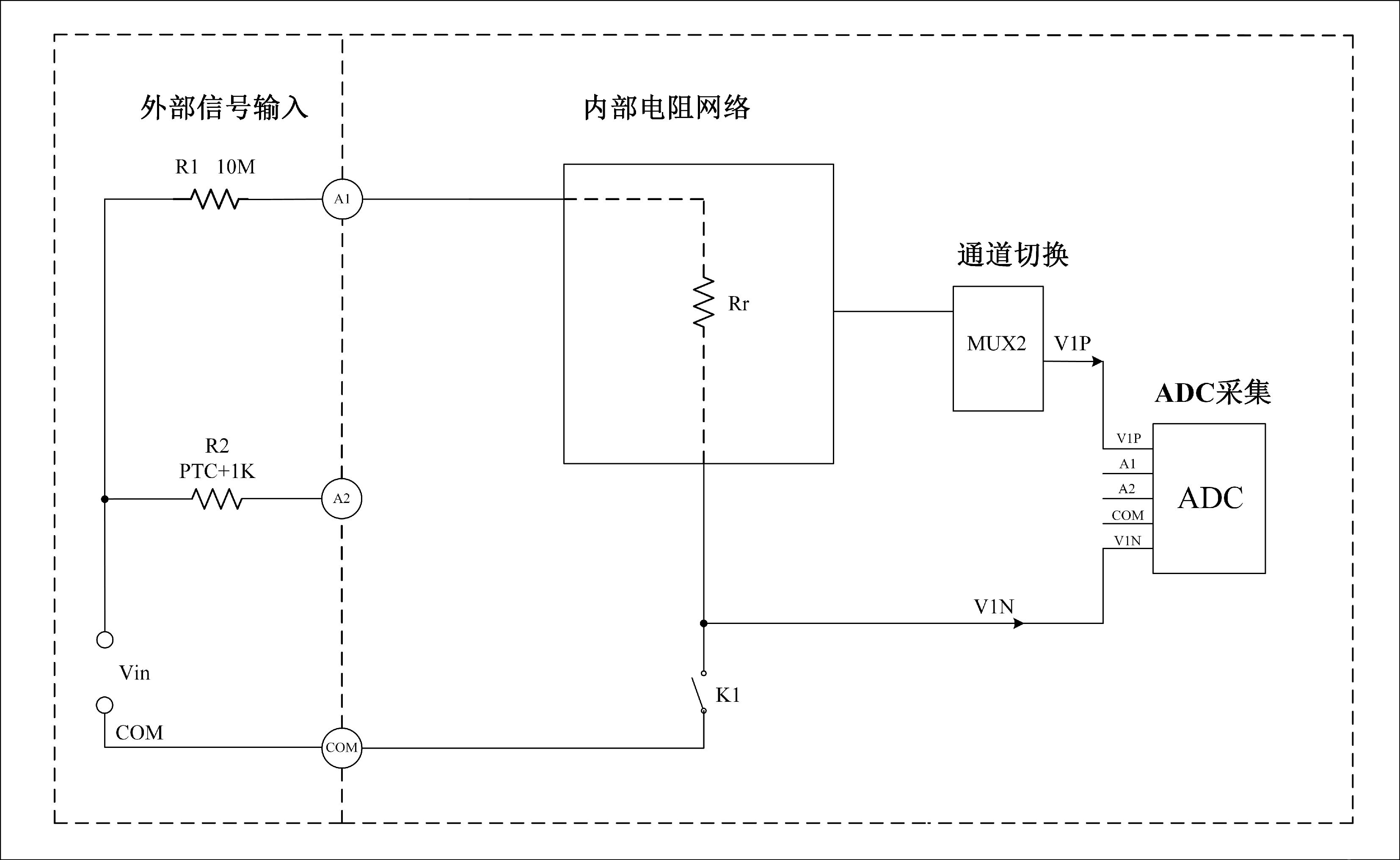
Figure 2. Schematic diagram of voltage measurement connections
Principle of voltage measurement
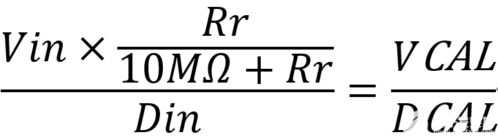
Figure 2 is a schematic diagram of the internal switch network connection of the chip. The principle is to divide the voltage from the external input voltage signal through the 10M resistor to the internal resistor network, and close the switch K1 to connect to COM to form a loop. Voltage range measurements are generally calibrated. The internal resistance network will switch between different voltage levels. One principle is to make the voltage divider on Rr as large as possible, and then use the 24-bit high-precision ADC inside the chip to measure the voltage across the Rr resistor to obtain the code value Din, and then according to The principle of dividing the voltage of the series circuit can solve the voltage value of Vin.
The derivation is as follows:
Epilogue
SD7890 chip cleverly uses the resistance network inside the chip to realize the measurement of resistance and voltage, and the peripheral circuit is simple, the anti-interference ability is strong, the measurement accuracy and measurement reliability are improved, and the resistance and voltage measurement accuracy is within ±0.5% (all The measurements are all proportional measurements to offset the errors existing in the system), and at the same time, it can reduce the production cost of the manufacturer and improve the production efficiency.